
 Problems in Semiconductor Manufacturing
Graphical User Interface for IC Tools
During the past several years, work in the Statistics group has led to many new tools for the analysis of spatial data collected during the manufacture of silicon integrated circuits. Developed by Mark Hansen, David James and Daryl Pregibon, these tools have increased the productivity of product and process engineers considerably. Recently, Lorraine Denby and David James designed a graphical user interface to make these tools more accessible and easier to use. The GUI is easy to learn, provides easy and flexible use of the tools, and can guide and engineer through analyses. The data in typical applications is voluminous and comes from various stages of the manufacturing process; the GUI provides easy integration of all the different types of data. A certain degree of interaction can be achieved through some simple Java applets written by Mark Hansen. If you have a Java-enabled browser, you are invited to try out the waferApplet.
Monitoring Wafer Map Data from Integrated Circuit Fabrication Processes for Spatially Clustered Defects
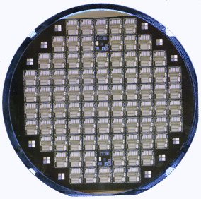
Quality control in integrated circuit (IC) fabrication has traditionally been based on overall summary data such as lot or wafer yield. These measures are adequate if the defective IC's are distributed randomly both within and across wafers in a lot. In practice, however, the defects often occur in clusters or display other systematic patterns. In general, these spatially clustered defects have assignable causes that can be traced to individual machines or to a series of process steps that did not meet specified requirements. Mark Hansen, David Friedman and Vijay Nair have developed methods for routinely monitoring probe test data at the wafer map level to detect the presence of spatial clustering. They have studied the statistical properties of a family of monitoring statistics under various null and alternative situations of interest, and have applied the resulting methodology to manufacturing data.
Click here for a technical report describing the project.
Model-Free Estimation of Some Yield Metrics in Integrated Circuit Fabrication
Mark Hansen, David Friedman, Vijay Nair and David James have developed a new, model-free method for estimating analogs of two important metrics used to track the integrated circuit fabrication process: $D_0$, the random defect density, and $Y_0$, a measure of (the lack of) defect clustering. Unlike previous methods discussed in the literature, their approach makes extensive use of the spatial information in wafer map data to estimate these metrics at the wafer level. Simulation studies show that their procedure is superior to the time-honored windowing technique.
Click here for a technical report describing the project.